- 您现在的位置:买卖IC网 > Sheet目录465 > IXTV200N10T (IXYS)MOSFET N-CH 100V 200A PLUS220
IXTV200N10T
IXTV200N10TS
Symbol Test Conditions
(T J = 25 ° C, unless otherwise specified)
Characteristic Values
Min. Typ. Max.
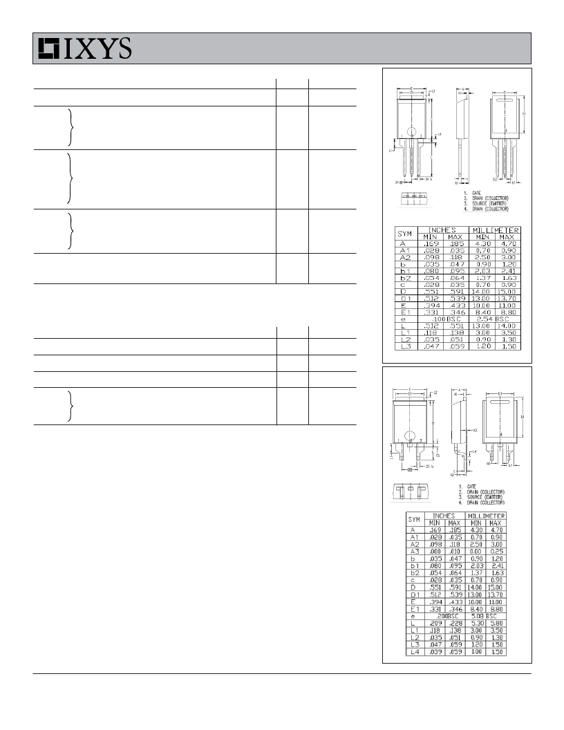
PLUS220 (IXTV) Outline
g fs
C iss
C oss
C rss
t d(on)
t r
t d(off)
t f
Q g(on)
Q gs
Q gd
V DS = 10V, I D = 60A, Note 1
V GS = 0V, V DS = 25V, f = 1MHz
Resistive Switching Times
V GS = 10V, V DS = 0.5 ? V DSS , I D = 50A
R G = 3.3 Ω (External)
V GS = 10V, V DS = 0.5 ? V DSS , I D = 50A
60
96
9400
1087
140
35
31
45
34
152
47
47
S
pF
pF
pF
ns
ns
ns
ns
nC
nC
nC
R thJC
0.27 ° C/W
R thCH
PLUS220
0.21
° C/W
Source-Drain Diode
Symbol Test Conditions
(T J = 25 ° C, unless otherwise specified)
Characteristic Values
Min. Typ. Max.
I S
V GS = 0V
200
A
I SM
V SD
t rr
Q RM
I RM
Repetitive, Pulse width limited by T JM
I F = 50A, V GS = 0V, Note 1
I F = 100A, V GS = 0V,-di/dt = 100A/ μ s
V R = 50V
76
205
5.4
500
1.0
A
V
ns
nC
A
PLUS220SMD (IXTV_S) Outline
Notes: 1. Pulse test, t ≤ 300 μ s; duty cycle, d ≤ 2%.
2. On through-hole packages, R DS(on) Kelvin test contact
location must be 5mm or less from the package body.
IXYS reserves the right to change limits, test conditions, and dimensions.
IXYS MOSFETs and IGBTs are covered
4,835,592
4,931,844
5,049,961
5,237,481
6,162,665
6,404,065 B1
6,683,344 6,727,585 7,005,734 B2
7,157,338B2
by one or more of the following U.S. patents: 4,850,072
5,017,508
5,063,307
5,381,025
6,259,123 B1
6,534,343
6,710,405 B2 6,759,692 7,063,975 B2
4,881,106
5,034,796
5,187,117
5,486,715
6,306,728 B1
6,583,505
6,710,463
6,771,478 B2 7,071,537
发布紧急采购,3分钟左右您将得到回复。
相关PDF资料
IXTV22N50PS
MOSFET N-CH 500V 22A PLUS220-SMD
IXTV22N60PS
MOSFET N-CH 600V 22A PLUS220-SMD
IXTV230N085TS
MOSFET N-CH 85V 230A PLUS220SMD
IXTV250N075T
MOSFET N-CH 75V 250A PLUS220
IXTV280N055TS
MOSFET N-CH 55V 280A PLUS220SMD
IXTV36N50PS
MOSFET N-CH 500V 36A PLUS220-SMD
IXTV96N25T
MOSFET N-CH 250V 96A PLUS220
IXTX110N20L2
MOSFET N-CH 200V 110A PLUS247
相关代理商/技术参数
IXTV200N10TS
功能描述:MOSFET 200 Amps 100V 5.4 Rds RoHS:否 制造商:STMicroelectronics 晶体管极性:N-Channel 汲极/源极击穿电压:650 V 闸/源击穿电压:25 V 漏极连续电流:130 A 电阻汲极/源极 RDS(导通):0.014 Ohms 配置:Single 最大工作温度: 安装风格:Through Hole 封装 / 箱体:Max247 封装:Tube
IXTV22N50P
功能描述:MOSFET 22.0 Amps 500 V 0.27 Ohm Rds RoHS:否 制造商:STMicroelectronics 晶体管极性:N-Channel 汲极/源极击穿电压:650 V 闸/源击穿电压:25 V 漏极连续电流:130 A 电阻汲极/源极 RDS(导通):0.014 Ohms 配置:Single 最大工作温度: 安装风格:Through Hole 封装 / 箱体:Max247 封装:Tube
IXTV22N50PS
功能描述:MOSFET 22.0 Amps 500 V 0.27 Ohm Rds RoHS:否 制造商:STMicroelectronics 晶体管极性:N-Channel 汲极/源极击穿电压:650 V 闸/源击穿电压:25 V 漏极连续电流:130 A 电阻汲极/源极 RDS(导通):0.014 Ohms 配置:Single 最大工作温度: 安装风格:Through Hole 封装 / 箱体:Max247 封装:Tube
IXTV22N60P
功能描述:MOSFET 22.0 Amps 600 V 0.33 Ohm Rds RoHS:否 制造商:STMicroelectronics 晶体管极性:N-Channel 汲极/源极击穿电压:650 V 闸/源击穿电压:25 V 漏极连续电流:130 A 电阻汲极/源极 RDS(导通):0.014 Ohms 配置:Single 最大工作温度: 安装风格:Through Hole 封装 / 箱体:Max247 封装:Tube
IXTV22N60PS
功能描述:MOSFET 22.0 Amps 600 V 0.33 Ohm Rds RoHS:否 制造商:STMicroelectronics 晶体管极性:N-Channel 汲极/源极击穿电压:650 V 闸/源击穿电压:25 V 漏极连续电流:130 A 电阻汲极/源极 RDS(导通):0.014 Ohms 配置:Single 最大工作温度: 安装风格:Through Hole 封装 / 箱体:Max247 封装:Tube
IXTV230N085T
功能描述:MOSFET 230 Amps 85V 4.1 Rds RoHS:否 制造商:STMicroelectronics 晶体管极性:N-Channel 汲极/源极击穿电压:650 V 闸/源击穿电压:25 V 漏极连续电流:130 A 电阻汲极/源极 RDS(导通):0.014 Ohms 配置:Single 最大工作温度: 安装风格:Through Hole 封装 / 箱体:Max247 封装:Tube
IXTV230N085TS
功能描述:MOSFET 230 Amps 85V 4.1 Rds RoHS:否 制造商:STMicroelectronics 晶体管极性:N-Channel 汲极/源极击穿电压:650 V 闸/源击穿电压:25 V 漏极连续电流:130 A 电阻汲极/源极 RDS(导通):0.014 Ohms 配置:Single 最大工作温度: 安装风格:Through Hole 封装 / 箱体:Max247 封装:Tube
IXTV250N075T
功能描述:MOSFET 250 Amps 75V 3.4 Rds RoHS:否 制造商:STMicroelectronics 晶体管极性:N-Channel 汲极/源极击穿电压:650 V 闸/源击穿电压:25 V 漏极连续电流:130 A 电阻汲极/源极 RDS(导通):0.014 Ohms 配置:Single 最大工作温度: 安装风格:Through Hole 封装 / 箱体:Max247 封装:Tube
